I took another pass at the DX7s tonight. I soldered a 0.1″ breakaway header to one of the RAM chips, which made hooking the logic analyser up a lot neater, as seen below:
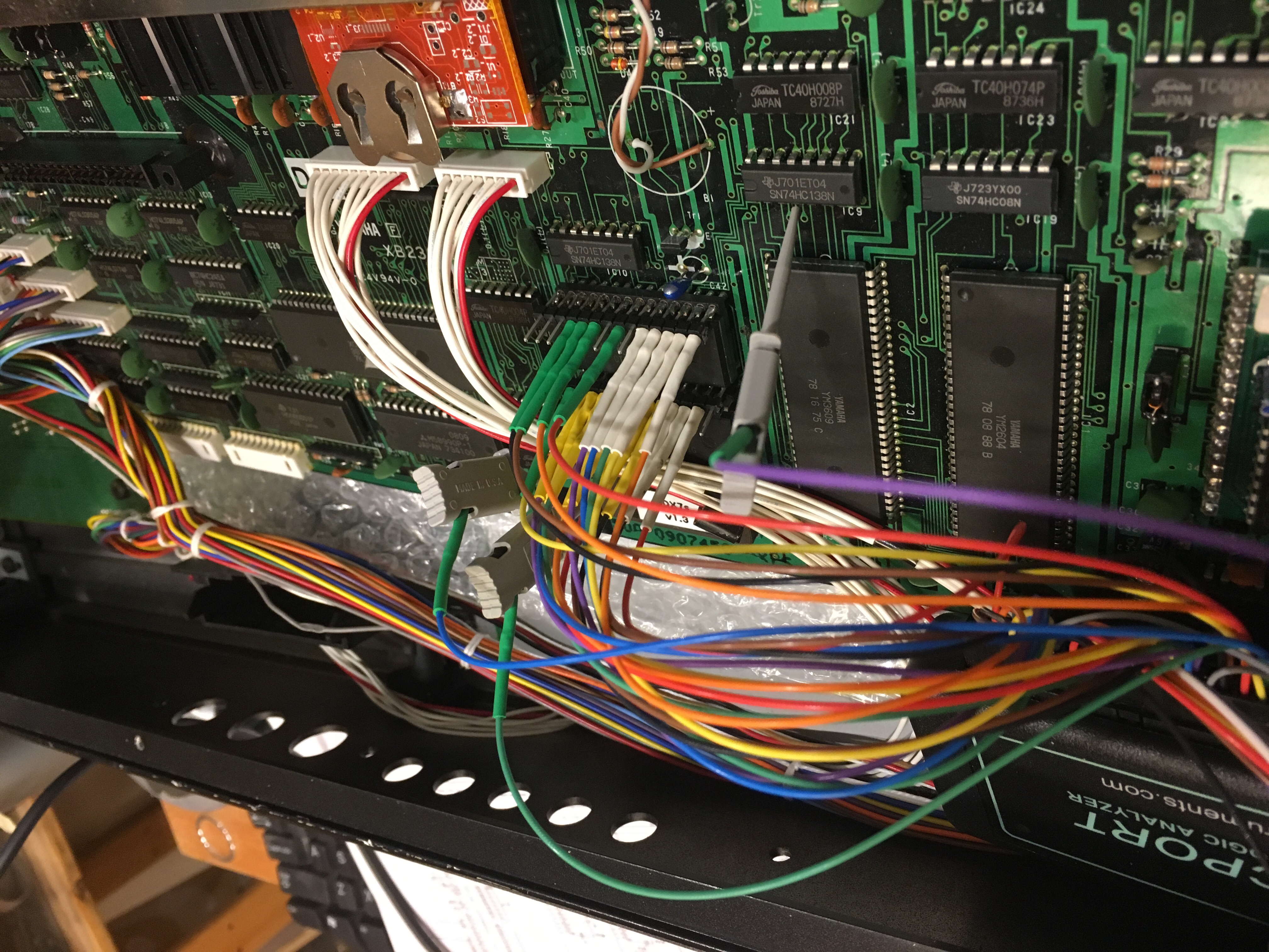
Better Logic Analyser Hookups
I went over the same steps that I did previously. I got to the point where RTS instruction was bad. I then started probing around the chip selects to see if something was selected that should not have been. I was thinking that the bus must have been driven by some other peripheral in error.
What I found instead was that the chip select for the RAM did not seem right. It seemed to be toggling but not at the right points to read from the RAM successfully. I traced the write to top of the stack from the JSR instruction, and the !CS1 line was not asserting low to write to the RAM.
Next I dragged out the scope and checked !CS1. It was toggling between 1 and 2V which seemed a little weird (not sure how I missed this bad signal the first time through). Looking at the schematic to find the origin of the signal revealed this:
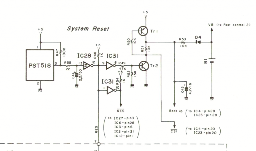
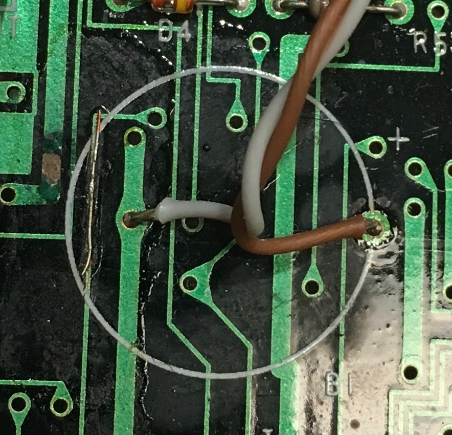
So !CS1 was part of the reset circuit, and should be low ALL THE TIME in normal run mode. The next step was to do a bit of continuity checking…. it turns out there was none! Following the trace revealed this (after some scraping away of the solder mask):
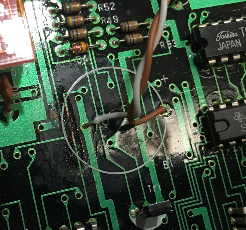
And here is the fix. This was somewhat obvious in retrospect. The battery leaked on to the board and corroded the trace, but it happened under the solder mask, so it wasn’t readily apparent. After this fix below, the DX7s just started up like normal.
So this was a lot of work, but I got to get more practice with the logic analyser, IDA Pro, and disassembling some code. I’ve got an updated rom one the board to boot! (no pun intended!)