For the past little while I’ve been debugging my Yamaha DX7s FM Synthesizer. It is still not working, but I’m having fun hacking on it. The DX7s has the dreaded ’88’ problem. That is what the LEDs display on the front panel… and nothing else works. I’d tried to fix this DX7s before, but had no documentation at the time. Recently I found a schematic online, so I thought I’d try again.
The typical ’88’ problem is bad clocks. I ‘scoped all the clock lines and everything looked fine. After looking at the schematic and the 6303 processor manual, it turned out there was supposed to be a GPIO output at 512KHz that clocks one of the sub-processors. It was not clocking, so obviously something was not copacetic.
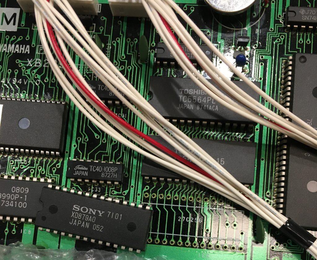
Scoping all the clock and data lines, chip selects etc. Seemed fine. The unit was running… but it wasn’t. I checked all the address and data lines for continuity, that was ok too. The next thing I did was pull the ROM (27c256, 32Kx8) and the RAM (2 x 8Kx8). I soldered in some machined sockets and replaced the chips, but not before reading out ROM (it looked ok)
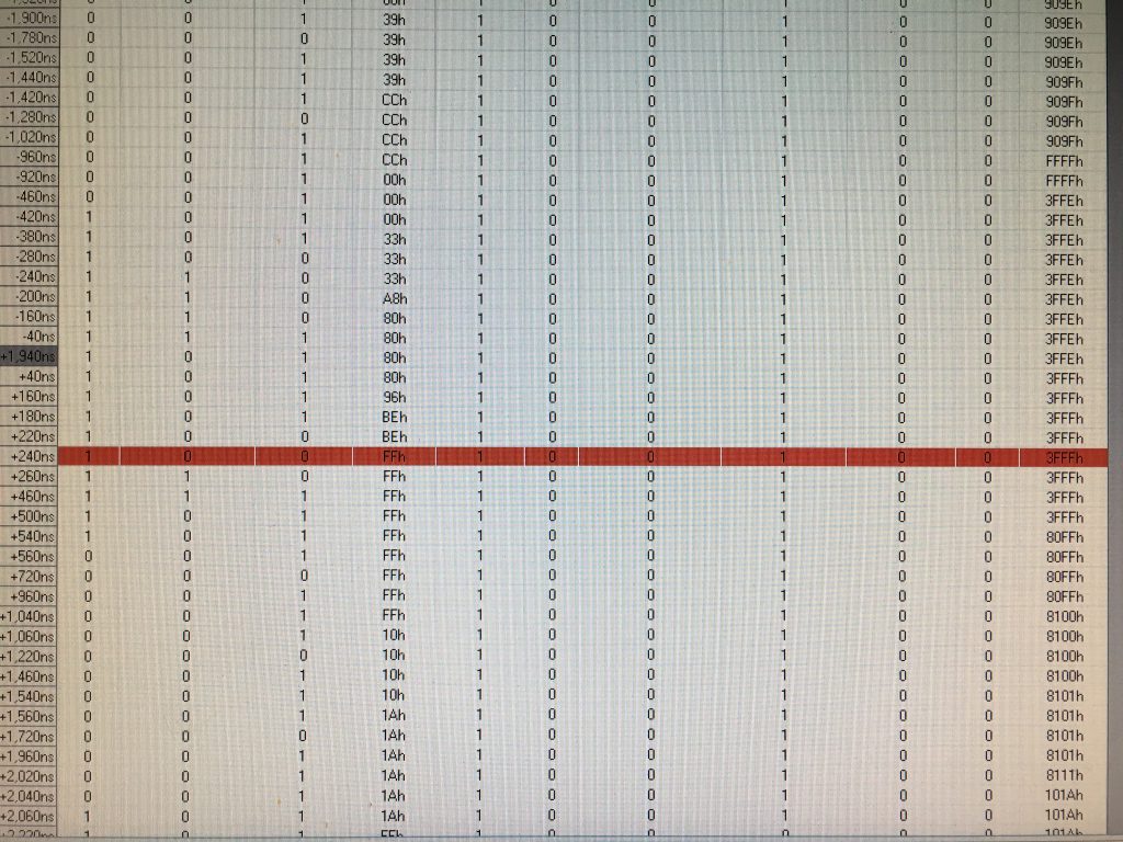
Next I put on a 34 channel USB logic analyser. This is the first time I’ve used one of these units, and it worked quite well. One of the more useful things that the micro in the DX7 (6303) has (but is unused in the circuit) is an #LIR (load instruction register) pin. When this is low the opcode of the instruction is on the data bus… cool.
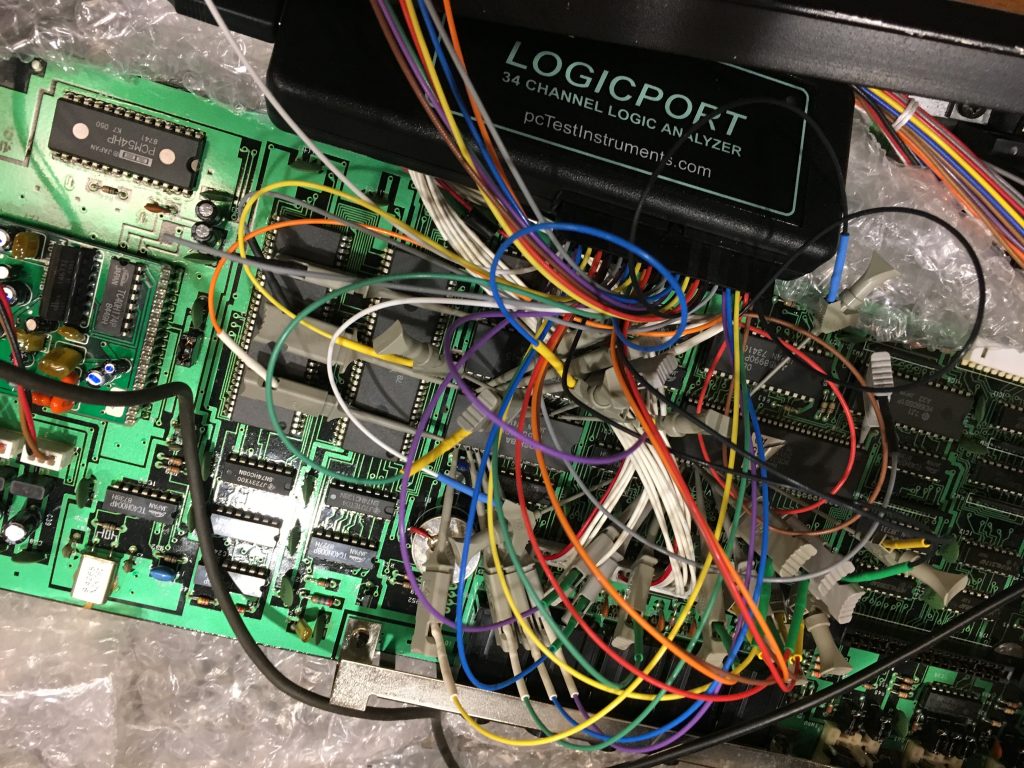
When I looked at the rom dump, the reset vector (@FFFE-FFFF) pointed to 8000, the start of the ROM. I set up a trigger on addr 8000, and watched the opcodes go by. It still looked like this thing was running. I noticed that there was a reboot loop. When the code got to addr 909E, it then went back to 8000 again. This did not seem right. So time to pull out IDA Pro and see what was going on.
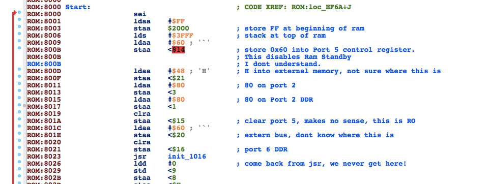
The start of the code sets the stack pointer, sets up some ports and and JSRs to some init routines:
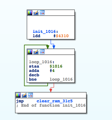
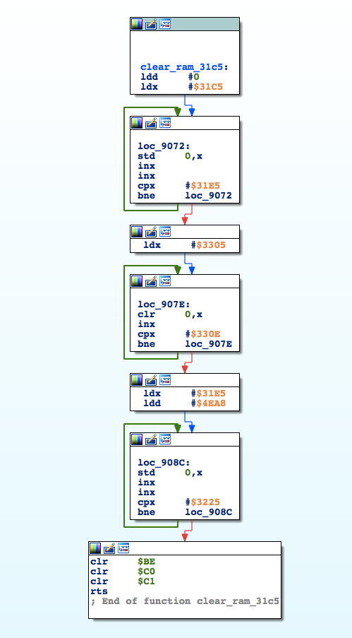
The RTS instruction is where the processor goes off the rails. This is where the code reboots, instead of returning to address 8026. Pulling out the logic analyser again shows that when the RTS instruction executes, it tries to pull the return address from memory. 0x80 is pulled out of 3FFE (correct), and 0xFF is pulled from 3FFF. Whiskey Tango Foxtrot?
So…. Something is bad. RAM is my guess, but I tried swapping the existing chips to no avail (I only put the logic analyser on one of them, since setup is a pain). I’ve got new RAM chips on order, plus a bunch of the “glue” address select logic chips, in case timing is out of spec, and a new processor from ebay. So at this point it is time to pack this thing back up and wait for parts. More info soon, I hope. This work is really not cost effective, since a new keyboard is $500-$1000 bucks. But from a hobby perspective, this has been a blast!
Update Feb 20th.
The new RAM chips arrived from DigiKey. I swapped them. No luck. Next steps are to desolder the 64 pin 6303, and solder pin headers on to one of the new RAM chips to make the logic analyser hookup easier. I’m still confused as to what is going on. Something must be driving the data bus that is not supposed to. A bad processor?, something else on the bus that somehow got its enable line set? Time to spend more quality time with the logic analyser and scope. Too bad I’m not a hardware guy, but then this wouldn’t be a hobby, would it?